In the nearly two decades since the SD Association (SDA) introduced its first memory cards, SD and microSD memory cards have cycled through numerous evolutions and industry trends.
Now, the microSD Express memory card takes a giant step forward by giving the microSD form factor PCIe® and NVMe™ capabilities alongside the legacy SD interface. This move opens new opportunities for mobile devices, gaming, drones, Internet of Things (IoT) and other applications to use the highest-performance removable memory cards.
microSD Express exists to meet users’ burgeoning and demanding storage needs. Faster speeds are essential for high-performance content, including speed-hungry applications running on cards and mobile computing devices; real memory expansion for mobile computing; ever-evolving gaming systems; multi-channel IoT devices; multi-processing automotive storage needs; high-performance mobile phones; super-slow-motion video; RAW continuous-burst mode photography; 8K video capture and playback; 360-degree video; and faster download/upload from high-capacity cards. These applications, along with evolving technology trends, signal a clear demand for memory cards with the high-performance sequential and random access provided by SD Express.
While there are a variety of storage standards out there, what makes the PCIe/NVMe standards the best option for microSD Express (in addition to its given high sequential performance levels)?

NVMe Advantages
To understand NVMe’s upsides, a brief history lesson is needed. For years, SAS and SATA were the computing industry’s chosen standards for hard drive interfaces, tapes, floppy drives and DVDs, from data centers up to mobile computing. Because of this, SSDs were initially equipped to support the SAS and SATA protocols; those SSDs continue to be widely accepted and used for their performance and value.
However, these solutions also come with the overhead of SAS and SATA command translation layers, and bandwidth challenges in supporting the performance demands of applications using SSDs. With increasing deployments of SSD technology in all computing environments, along with the wider adoption of flash memory-based technologies, a new combination of a protocol standard and an interface was needed.
For flash memory-based SSDs, the ideal protocol and interface combination did not exist until several years ago, when the NVMe technology standard coupled with a PCIe interface first appeared.
NVMe is the first interface specification to take full advantage of an SSD’s strengths and potential. Further, NVMe, in combination with PCIe, defines new usage modes and data types, such as borrowing memory from the system, creating new semantics, and integrating with the network, to name a few.
NVMe comes with standard drivers for ease of use, and provides a high-bandwidth, low-latency framework for SSDs. NVMe’s success is primarily due to the removal of translation commands that would normally occur in the SATA or SAS controller. NVMe removes these controllers’ latency, as well as software latency, and can double — and sometimes triple — sequential throughput rates by eliminating processing times and the constricting SATA or SAS pipeline.
Another performance and scale feature of the NVMe is Multiple Queues, which support a large number of deep queues and commands per queue. Numerous studies show that an NVMe-based interface may achieve more than a 30 percent improvement in random performance over SCSI-based interfaces. These capabilities drove expanded NVMe adoption when hyperscale environments became popular. The same advantage may be utilized in any future multiprocessing systems that are widely evolved in all market segments, including mobile devices.
These new scale-out architectures mean NVMe has clear advantages in highly scalable deployments. The SCSI bottleneck of middle-layer translations struggled to support simultaneous IOs and multiple hosts, making SAS difficult to expand effectively, but now, with Multitenant and Multiple Queues features, NVMe removes the bottleneck and seamlessly supports these environments.
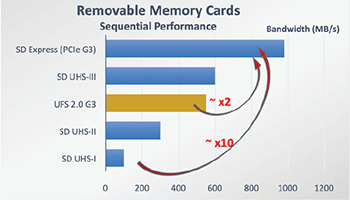
The UFS specification developed by JEDEC uses the abovementioned SCSI command layer, with a few added new commands unique to UFS specification.
PCIe supplements NVMe’s benefits, offering four main advantages: differential interface; 128b/130b encoding; power consumption; and AC coupling.
The Differential Interface
The legacy SD UHS-I interface have a single-ended type of signal lines, similar to eMMC. The PCIe Gen3 uses a differential interface of serial communication, similar to SD UHS-II and UFS. There are several known benefits of differential interface:
- Resistance to incoming electromagnetic interference (EMI) and crosstalk;
- Reduction of outgoing EMI and crosstalk;
- Lower signal-to-noise ratio (SNR); and
- Simpler high/low states detection.
The 128b/130b Encoding Advantage
The PCIe Gen 3 uses a 128b/130b block encoding/decoding scheme, which is different from the 8B/10B scheme used in UFS, SATA and the earlier PCIe Gen1 and PCIe Gen 2. The 130-bit block contains a 2-bit sync header and 128-bit data payload. While in 8b/10b, for every 10 bits, 2 bits are used for sync and 8 are payload, the overhead in PCIe Gen 3 is much smaller than in the other mentioned protocols. This means the actual valid data transfer for the same block of bits will be significantly more efficient with PCIe.
It also means when transferring a certain amount of data, fewer bits need to be sent on the communication line, which will directly affect the total consumed power associated with the physical circuitry in a chip required to implement physical layer function (PHY) for the same amount of data transfer.
The Power Consumption Advantages
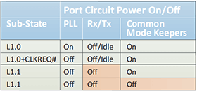
PCIe 3.1, which microSD Express uses, includes the new low-power sub-states L1.0, L1.1 and L1.2, which were added on top of L0 to L3, introduced earlier in PCIe 3.0. The new sub-states enabled additional low power states that ensure the best system optimization of low power versus recovery times.

The legacy SD interface – including UHS-I – consists of six single-ended signals that may operate either in 3.3v or 1.8v logic levels. The 1.8v signaling allows lower power consumption than the 3.3v. The differential interfaces, introduced by the SD UHS-II/III interfaces (0.14-0.28v), as well as the PCIe interface (0.25-1.2v), introduced with SD Express, allow a significantly lower voltage swing, which reduces the consumed power contributed by the PHY during data transfer.
Because the transfer rate is faster, the bottom line is that the new high speed interface will be much more energy-efficient than the legacy SD UHS-I interface, because the system can transfer the same amount of data in less time and stay in standby mode longer.
The Advantages of AC coupling over DC Coupling
There are two commonly used interface coupling methods: AC and DC. The PCIe physical interface has the former, which provides many benefits, such as level shifting, removing common-mode errors, and protecting against input-voltage fault conditions. AC coupling has advantages mainly in connections between different units using connectors and cables, such as removable memory cards.
Another advantage is realized when the SD memory card socket is wired, as in automotive and industrial applications, IoT and more. In automotive, the differential signals are always AC-coupled to protect the car’s battery voltage from shorting out. A universal requirement for any signal entering the wiring harness is that it must withstand a short-to-battery voltage without damage.
With an AC-coupled differential interface link, there is only a brief pulse of high current as the coupling capacitors are charged to the battery voltage. The peak amplitude of the current is a function of the actual impedance of the short. The duration of the spike is a function of the coupling capacitance and the protection structure of the differential signal input and output.
microSD Express: Boosted by PCIe and NVMe
Choosing microSD Express or SD Express for all removable card needs means choosing PCIe and NVMe – the proven worldwide standards that are the leading specifications for flash memory interfacing. SD Express memory cards now benefit from these two standards’ continued research, development and long-term roadmaps.
With these standards included in the new microSD Express memory card, this popular SD form factor now can reach SSD levels of performance, enabling exceptional user experience for multi-processing environments. These protocols create a host of new opportunities for users, and are expected to serve the memory-interfacing ecosystem for the next decade and beyond.
Yosi Pinto is chairman of the SD Association. Pinto can be reached at Yosi.Pinto@wdc.com
PCI Express® is a registered trademark of PCI-SIG®.
NVM Express™ and NVMe™ are trademarks of NVM Express, Inc.
© SD Association. All rights reserved. SD, microSD, SDHC, microSDHC, SDXC, microSDXC, SDUC, microSDUC Logos are trademarks licensed by SD-3C LLC.


